4 Diodes _ Rectifiers
Diodes & Rectifiers
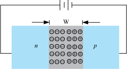
p–n Junction Formation
- A thin p-type semi-conductor wafer is considered. A part of it is converted into n-Si by adding a small quantity of pentavalent impurity.
- Wafer now contains a p-region and n-region and a metallurgical junction between p-, and n-region.
- n-type semi-conductor has more concentration of electrons than hole and p-type semi-conductor has more concentration of holes than electron. Therefore, the holes diffuse from p-side to n-side and electrons diffuse from n-side to p-side.
- When an electron diffuses from n to p, it leaves behind it an ionised donor on n-side. The ionised donor (+ ve charge) is immobile as it is bounded by the surrounding atoms.
- Therefore, a layer of positive charge is developed on n-side of the junction.
- Similarly, a layer of negative charge is developed on the p-side.
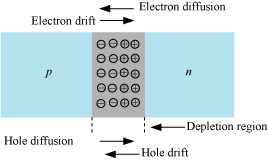
- This space-charge region on either side of the junction together is called depletion region.
- The positive space-charge region on n-side of the junction and negative space-charge region on p-side of the junction, appearing as electric field, is developed and directed from + ve charge to − ve charge.
- Due to the field, an electron from p-side moves to n-side and a hole from n-side of the junction moves to p-side.
- The motion of charge carriers due to electric field is called drift current and is opposite in direction to the diffusion current.
- Initially, diffusion current is large and drift current is small. As diffusion continues, the space charge regions on either side of the junction extends, thereby increasing the electric field strength and hence drift current. The process continues until the diffusion current is equal to drift current.
- Thus, a p–n junction is formed. Under equilibrium, there is no net current.
- Loss of electrons from the n-region and gain of electron by the p-region causes a difference of potential across the junction of two regions. This potential tends to prevent the movement of electron from n to p region. Therefore, it is called a barrier potential.
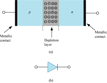
Semi-conductor Diode
- A semi-conductor diode is basically ap–n junction with metallic contacts provided at the ends for the application of an external voltage.
- A p–n junction diode is symbolically represented as shown in the figure below.
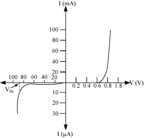
p–n junction diode under forward bias
- p-side is connected to positive terminal and n-side to the negative terminal.
- Applied voltage drops across the depletion region.
- Direction of applied voltage (V) is opposite to the build in potential (V0).
- As the depletion layer width decreases, the barrier height is reduced.
- Effective barrier height under forward bias is (V0− V).

- Electron inn-region moves towards the p–n junction and holes in p-region move towards the junction. The width of the depletion layer decreases and hence, it offers less resistance.
- Diffusion of majority carriers takes place across the junction.
This leads to forward current.
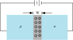
p–n junction diode under reverse bias
- Positive terminal of battery is connected ton-side and negative terminal to p-side.
- Reverse bias supports the potential barrier. Therefore, the barrier height increases and the width of depletion region also increases.
- Effective barrier height under reverse bias is (V0+ V).

- No conduction across the junction due to majority carriers; few minority carriers cross the junction after being accelerated by high reverse bias voltage
- This constitutes a current that flows in opposite direction − celled reverse current.
Rectifier
It is a device used for converting alternating current/voltage into direct current/voltage.
- Half wave rectifier is based on the principle that the resistance of p–n junction becomes low when it is forward biased and becomes high when reverse biased.
- When voltage at A is positive, it conducts; and when negative, it does not conduct.
- Therefore,in the positive half cycle of ac, there is a current through RL and we obtain O/P voltage.
- In the negative half cycle, there is no current.
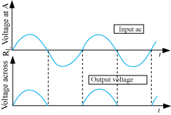
- Since the rectified output of this circuit is only for half of i/p ac wave, it is called half wave rectifier.
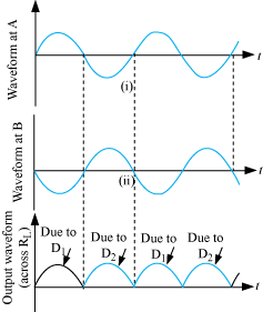
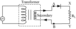
Full −wave rectifier
- Two diodes are used to give rectified O/P corresponding to both positive as well as negative half cycles.
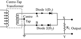
- When voltage at A with respect to the centre tap is positive, and the voltage at B is negative. Then, D1 is forward biased and D2 is reversed biased. Hence, D1 conducts and D2 does not.
- When voltage of A becomes negative, then B becomes + ve. Therefore, D1does not conduct and D2 Hence, we obtain output voltage during both the positive as well as negative half of cycle.