5 Special Purpose p-n Junction Diodes
Special Purpose p-n Junction Diodes
Zener Diode
- It can operate in the reverse breakdown voltage region continuously without being damaged.
- Symbol

- It is a heavily doped p–n junction. Due to this, depletion region formed is very thin and the electric field of the junction is extremely high, even for a small reverse bias voltage.
- The I−V characteristics of a zener diode are shown in the figure below.
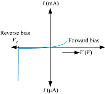
- It is widely used to regulate the voltage across the circuit.
Zener Diode as Voltage Regulator
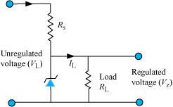
- After the break down voltage, small change in voltage across the zener diode produces a large change in current through the circuit.
- If voltage is increased beyond zener voltage, then the resistance of the zener diode drops considerably.
- Zener diode and a resistor are connected to a fluctuating dc supply such that the zener diode is reverse biased.
- When the voltage across the diode tends to increase, the current through the diode rises out of proportion and causes a sufficient increase in voltage drop across the resistor. Therefore, the O/P voltage lowers back to normal.
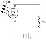
Photodiode
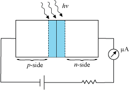
- A junction diode made from light sensitive semi-conductor is called a photodiode.
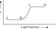
- Current AB that flows when no light is incident is called dark current.
- When photons of light having energy hνfall on the photodiode, more electrons from valence band move to the conduction band, provided hv is greater than forbidden energy gap.
- The current in the circuit increases. As the intensity of light is increased, the current goes on increasing as in part BC.
- When the current does not increase with the increase in intensity of light, the photodiode is said to be saturated. Portion CD of the graph represents saturated current.
Light Emitting Diodes (LEDs)
- All junction diodes emit some light when forward biased.
- Junction diode is made of gallium arsenide (GaAs). The energy is released in infrared region while those made of gallium arsenide phosphide (GaAsP) emit radiation in visible region. They are called LEDs.
- The most important part of a LED is the p–n junction. The junction acts as a barrier to the flow of electrons between the p and n regions. Only when sufficient voltage is applied to the LED, the electrons cross the junction into the p-region and current flows through it.
- Diode is encapsulated with a transparent cover so that emitted light can come out.
- LEDs are biased such that the light emitting efficiency is maximum.
- Semi-conductor used to fabricate visible LEDs must have at least 1.8 eV band gap.
- LEDs have low operational voltage and less power. They requires less warm-up time.
Solar Cell
- It is a semi-conductor device used to convert photons of solar light into electricity.
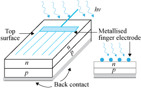
- It generates emf when solar radiations fall on the p–n junction.
- A p– Si wafer of about 300 μm is taken, over which a thin layer n− Si is grown on one side by diffusion process.
- The generation of emf by a solar cell when light falls on it is due to following three processes:
- Generation of e-h pairs due to light close to the junction
- Separation of electrons and holes due to electric field of the depletion region
- The electrons reaching the n-side are collected by the front contact and holes reaching p-side are collected by the back contact. Thus, p-side becomes positive and n-side becomes negative giving rise to photovoltage.
- Semi-conductors with band gap close to 1.5 eV are ideal materials for solar cell fabrication.